MCL-E-705G
Halogen Free, High Tg, High Elastic Modulus, Low CTE Multilayer Material
Product form
| CCL | MCL-E-705G |
| Prepreg | GEA-705G |
Applications
- Semiconductor packages. (FC-BGA, FC-CSP, PoP, SiP)
- HDI, PWB
- Thinner module, PWB
Features
- MCL-E-705G has low CTE values in X, Y directions and reduces warpage of package substrate significantly.
- MCL-E-705G (Type L) has lower CTE value (≤5ppm/℃).
- MCL-E-705G (Type LH) has lower CTE value (3ppm/℃).
- Well-suited for build-up construction.
Characteristics
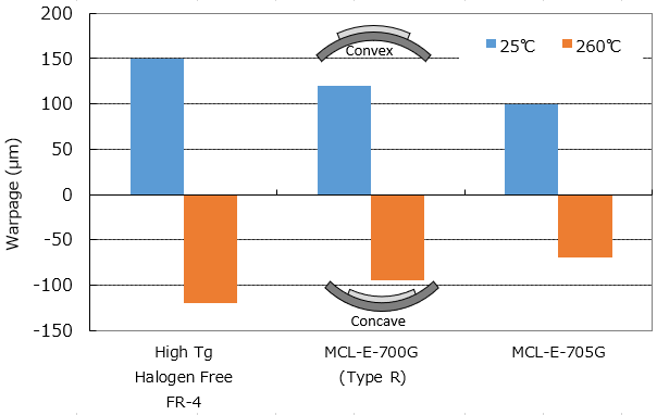
Warpage of FC-BGA

TEG Chip
- Chip size: 20mm×20mm
- Chip thickness: 0.725mm
- Bump diameter: 80 µm
- Bump pitch: 200 µm
TEG Substrate
- Package size: 35mm×35mm
- Core thickness: 0.4mm
- Build up thickness: 30 µm×2stack
- SR thickness: 20 µm

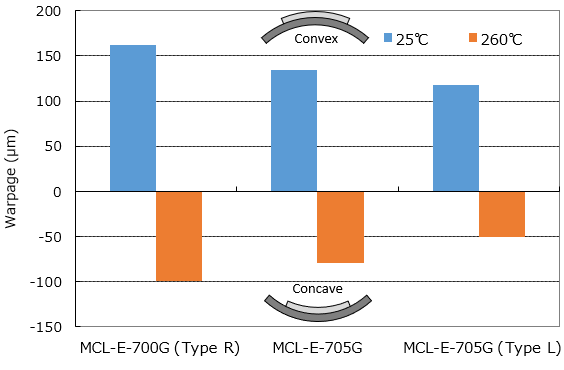
Warpage of PKG

TEG Substrate spec
- Size: 14mm×14mm
- Total thickness: 250 µm
- SR thickness: 20 µm (SR-7200G: Resonac)
- Prepreg thickness: 40 µm
- Core thickness: 110 µm

Copper Clad Laminate
| Item | Condition ※3 | Unit | Actual Value | Reference (IPC-TM-650) |
|||||
|---|---|---|---|---|---|---|---|---|---|
| MCL-E- 705G |
MCL-E- 705G (Type X) |
MCL-E- 705G (Type L) |
MCL-E- 705G (Type LH) |
||||||
| Tg | TMA method | A | ℃ | 250–270 | 2.4.24 | ||||
| DMA method | A | 295–305 | – | ||||||
| CTE ※1 | X (30–100℃) | A | ppm/℃ | 5–7 | 4–6 | 3–4 | 2.5–3.5 | – | |
| Y (30–100℃) | A | 5–7 | 4–6 | 3–4 | 2.5–3.5 | ||||
| Z※4 | (<Tg) | A | 10–15 | 2.4.24 | |||||
| (>Tg) | A | 70–100 | |||||||
| Solder Heat Resistance (260℃) | A | sec. | >300 | – | |||||
| T-260 (Without Copper) | A | min. | >60 | 2.4.24.1 | |||||
| T-288 (Without Copper) | A | >60 | |||||||
| Decomposition Temperature (TGA method 5% Weight Loss) | A | ℃ | 430–450 | 2.3.40 | |||||
| Heat Resistance for HDI Process (Semi-Additive) | 260℃ Reflow | cycles | >20 | – | |||||
| Copper Peel Strength | 12 µm | A | kN/m | 0.8–1.0 | 2.4.8 | ||||
| 18 µm | A | 0.9–1.1 | |||||||
| Surface Roughness (Ra) | A | µm | 2–3 | 2.2.17 | |||||
| Flexural Modulus (Lengthwise) ※4 | A | GPa | 32–34 | 33–35 | 34–36 | 37–39 | – | ||
| Dielectric Constant | 10GHz ※2 | A | – | 4.4–4.6 | 4.4–4.6 | 4.1–4.3 | 4.1–4.3 | – | |
| Dissipation Factor | 10GHz ※2 | A | – | 0.009–0.011 | – | ||||
| Volume Resistivity | C-96/40/90 | Ω・cm | 1×10¹⁴–1×10¹⁶ | 2.5.17 | |||||
| Surface Resistance | C-96/40/90 | Ω | 1×10¹³–1×10¹⁵ | ||||||
| Insulation Resistance | A | Ω | 1×10¹⁴–1×10¹⁶ | – | |||||
| D-2/100 | 1×10¹²–1×10¹⁴ | – | |||||||
※1 Heating Rate: 10℃/min.
※2 Measured by SPDR.
※3 Refer to “Condition Note”
※4 t0.8mm
※ Above data are experimental results and not guaranteed.
※2 Measured by SPDR.
※3 Refer to “Condition Note”
※4 t0.8mm
※ Above data are experimental results and not guaranteed.
Standard Specifications
Copper Clad Laminate
| Part Number | Type | Copper Foil Thickness | Thickness Code | Laminate Thickness |
|---|---|---|---|---|
| MCL-E- 705G |
– (L) |
2 µm, 3 µm, 12 µm (LP, PF) | T0.06 | 0.06mm |
| 12 µm 18 µm (STD) 2 µm 3 µm 12 µm (LP, PF) |
M0.06 | 0.06mm | ||
| 0.1 | 0.11mm | |||
| M0.11 | 0.10mm | |||
| M0.15 | 0.16mm | |||
| M0.22 | 0.21mm | |||
| 0.2 | 0.21mm | |||
| 0.31 | 0.31mm | |||
| 0.41 | 0.41mm | |||
| 0.51 | 0.52mm | |||
| 0.61 | 0.62mm | |||
| 0.71 | 0.72mm | |||
| 0.81 | 0.82mm | |||
| (X) | 12 µm 18 µm (STD) 2 µm 3 µm 12 µm (LP, PF) |
0.41 | 0.41mm | |
| 0.61 | 0.62mm | |||
| 0.81 | 0.82mm | |||
| (LH) | M0.06 | 0.06mm | ||
| 0.1 | 0.11mm | |||
| D0.15 | 0.16mm | |||
| 0.2 | 0.21mm | |||
| 0.26 | 0.26mm |
※1 STD: Standard copper foil, LP: Low profile copper foil, PF: Hitachi profile-free copper foil.
※2 STD: 12 µm, 18 µm; LP: 2 µm, 3 µm, 12 µm, 18 µm; PF:2 µm, 3 µm, 12 µm.
※3 “U” for 1-ply“; T” for 2-ply.
※4 The thickness means that of dielectric layer.
Prepreg
| Part Number | Type | Glass Cloth | Properties | |||
|---|---|---|---|---|---|---|
| Style | Resin Content (%) |
Dielectric Thickness after Lamination ※1 (mm) |
||||
| GEA-705G | – | ≦0.025 | (See GEA-705G (Type F) page for ultra thin, flat prepregs) | |||
| – | 0.025 | (1017N73) | 1017 | 73±2 | 0.025 | |
| 0.03 | (1027N73) | 1027 | 73±2 | 0.039 | ||
| 0.04 | (1037N73) | 1037 | 73±2 | 0.047 | ||
| 0.06 | (1078N65) | 1078 | 65±2 | 0.070 | ||
| 0.1 | (2116N58) | 2116 | 58±2 | 0.126 | ||
| (L) | 0.025 | (L1017N73) | 1017 | 73±2 | 0.025 | |
| 0.03 | (L1027N73) | 1027 | 73±2 | 0.039 | ||
| 0.04 | (L1037N73) | 1037 | 73±2 | 0.047 | ||
| 0.06 | (L1078N65) | 1078 | 65±2 | 0.070 | ||
| 0.1 | (L2116N58) | 2116 | 58±2 | 0.127 | ||
| Reference (IPC-TM-650) | 2.3.16 | ‐ | ||||
※1 The dielectric thickness after lamination is defined as the thickness of one sheet of prepreg when the resin flow is 0%. This value changes depending on the press condition or inner layer pattern.
Inquirer about product
Please subscribe our technology eNewsletter!
Inquiry about product
Please inquire about product, technology or samples from here.