PF-EL
Copper Foil for Fine Patterning
Product form
![]()
| Copper Foil | PF-EL |
Applications
- Semiconductor package substrates
- High density multi-layer PWB
Features
- PF-EL is a copper foil that is appropriate for fine line patterning with semi-additive process (SAP) using rough shapes of primer made with the copper profile.
- PF-EL has high peel strength for plating copper.
- High flexural modulus substrates with using prepregs.
Characteristics
Surface

PF-EL

PF-EL SP
Fine patterning with SAP

Design
L/S=10/10 µm with PF-EL
(Exposure LDⅠ)

Design
L/S=7/7 µm with PF-EL SP
(Exposure LDⅠ)

Design
L/S=5/5 µm with PF-EL SP
(Exposure Stepper)
Copper peel strength

※ Sample: MCL-E-770G (Type R), Copper foil 1.5 µm with plating copper 20 µm
Plating copper peel strength

※ Sample: MCL-E-770G (Type R), plating copper 20 µm
Fine patterning process


Standard Specifications
Copper Foil
![]()
| Part Number | Copper Foil Thickness (µm) |
Special Surface Treatment (µm) |
Roughness (µm) | Composition | Process |
|---|---|---|---|---|---|
| PF-EL-12 | 12 | 4 | Ra: 0.3–0.4 | 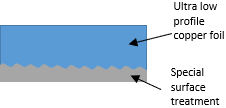 |
SAP ※1 |
| Rz: 1.5–2.5 | |||||
| PF-EL-3 | 3 | 2,4 | Ra: 0.3–0.5 | SAP ※1 MSAP ※2 |
|
| Rz: 1.5–2.5 | |||||
| PF-EL-2 | 2 | 2,4 | Ra: 0.3–0.5 | ||
| Rz: 1.5–2.5 | |||||
| PF-EL-1.5 | 1.5 | 2 | Ra: 0.3–0.5 | ||
| Rz: 1.5–2.5 | |||||
| PF-EL-1.5SP | 1.5 | 2 | Ra: 0.2–0.3 | ||
| Rz: 1.0–2.0 |
※1 After lamination of the material to the prepreg, the copper foil is etched out,and the special surface treatment with appropriate roughness made by a replica of the copper profile etched out remains on prepreg surface.This process is SAP using this replica.
※2 Semi additive process using thin copper foil as seed layer for having E’less copper +copper on both patterming and via plating purpose.
Inquirer about product
Please subscribe our technology eNewsletter!
Inquiry about product
Please inquire about product, technology or samples from here.