MCL-HS100
Halogen Free, High Tg, Low Transmission Loss, Low CTE Multilayer Material
Product form
| CCL | MCL-HS100 |
| Prepreg | GH-100 |
Applications
- Semiconductor packages. (FC-CSP, PoP, SiP)
- Thinner Module PWB
Features
- MCL-HS100 has hybrid properties of package and high speed materials.
- MCL-HS100 has low CTE value in X, Y directions and good dielectric property. (Dk 3.7, Df 0.0040 at 10GHz)
- MCL-HS100(Type D) achieved low dielectric constant (3.4 at 10GHz) and low dissipation factor (0.0025 at 10GHz) using low Dk glass.
- Well-suited for build-up construction.
Characteristics
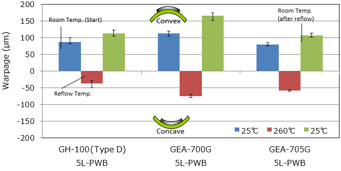
Warpage of coreless-5 layer

TEG Chip
- Package size: 14mm×14mm
- Chip size: 7.3mm×7.3mm
- Chip thickness: 150 µm
- Underfill thickness: 60 µm (CEL-C-3730-4)
TEG Substrate
- L1, 5: 12 µm Cu100%, L2, 3, 4: No copper, SR: –
Prepreg construction
- GH-100 (Type D) (: 1078, R.C.: 63%)×4ply
- GEA-700G (: 1078, R.C.: 66%)×4ply
- GEA-705G (: 1078, R.C.: 65%)×4ply

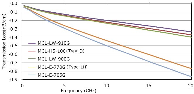
Transmission Loss

Measurement conditions
- Evaluation PWB: Strip-line
- Temperature & Humidity: 25℃/60%RH
- Characteristic impedance: Approx.50Ω
- Proofreading method: TRL (Thru-Reflect-Line)

- Trace width(w): 0.12–0.14mm
- Dielectric thickness(b): 0.25mm
- Trace thickness(t): 18 µm
Copper Clad Laminate
(t0.2, t0.4mm)
| Item | Condition ※3 | Unit | Actual Value | Reference (IPC-TM-650) |
|||
|---|---|---|---|---|---|---|---|
| MCL-HS100 | MCL-HS100 (Type D) | ||||||
| Tg | TMA method | A | ℃ | 240–260 | 2.4.24 | ||
| DMA method | A | 240–260 | – | ||||
| CTE ※1 | X (30–120℃) | A | ppm/℃ | 6–8 | – | ||
| Y (30–120℃) | 6–8 | ||||||
| Z | <Tg | A | 20–30 | 2.2.24 | |||
| >Tg | A | 130–180 | |||||
| Solder Heat Resistance (260℃) | A | sec. | >300 | – | |||
| T-260 (Without Copper) | A | min. | >60 | 2.4.24.1 | |||
| T-288 (Without Copper) | A | >60 | |||||
| Decomposition Temperature (TGA method 5% weight loss) | A | ℃ | 430–450 | 2.3.40 | |||
| Copper Peel Strength | 12 µm | A | kN/m | 0.7–0.9 | 2.2.8 | ||
| 18 µm | A | 0.8–1.0 | |||||
| Surface Roughness (Ra) | A | µm | 2–3 | 2.2.17 | |||
| Flexural Modulus (Lengthwise) | A | GPa | 23–28 | 2.4.4 | |||
| Dielectric Constant | 10GHz ※2 | A | – | 4.2–4.4 | 3.5–3.7 | IEC-62810 | |
| Dissipation Factor | 10GHz ※2 | A | – | 0.0050–0.0060 | 0.0025–0.0035 | ||
| Volume Resistivity | C-96/40/90 | Ω・cm | 1×10¹⁴–1×10¹⁶ | 2.5.17 | |||
| Surface Resistance | C-96/40/90 | Ω | 1×10¹³–1×10¹⁵ | ||||
| Insulation Resistance | A | Ω | 1×10¹⁴–1×10¹⁶ | – | |||
| D-2/100 | 1×10¹³–1×10¹⁵ | – | |||||
※1 Heating Rate: 10℃/min.
※2 Measured by Cavity Resonator.
※3 Refer to “Condition Note”
※ Above data are experimental results and not guaranteed.
Standard Specifications
Copper Clad Laminate
| Part Number | Type | Copper Foil Thickness | Code Name | Laminate Thickness |
|---|---|---|---|---|
| MCL-HS100 | – | 3 µm 12 µm (LP, HVLP) |
U0.04 | 0.04mm |
| 3 µm 12 µm 18 µm 35 µm (LP, RT, HVLP) |
M0.06 | 0.06mm | ||
| 0.1 | 0.10mm | |||
| 0.2 | 0.20mm | |||
| 0.41 | 0.40mm | |||
| (D) | 3 µm 12 µm (LP, HVLP) |
U0.04 | 0.04mm | |
| 3 µm 12 µm 18 µm 35 µm (LP, RT, HVLP) |
M0.06 | 0.06mm | ||
| 0.1 | 0.10mm | |||
| 0.2 | 0.20mm | |||
| 0.41 | 0.40mm |
※1 LP: Low profile copper foil, PF: Profile free copper foil.
※2 LP: 3 µm, 12 µm; RT: 18 µm, 35 µm; HVLP: 12 µm, 18 µm, 35 µm.
※3 The thickness means that of dielectric layer.
Prepreg
| Part Number | Type | Glass Cloth | Properties | |||
|---|---|---|---|---|---|---|
| Style | Resin Content (%) |
Dielectric Thickness after Lamination ※1 (mm) |
||||
| GH-100 | (D) | 0.025 | (See GH-200 (Type D) page for ultra thin, flat prepregs) | |||
| – | 0.03 | (1027N71) | 1027 | 71±2 | 0.042 | |
| 0.05 | (1037N71) | 1037 | 71±2 | 0.050 | ||
| 0.06 | (1078N61) | 1078 | 61±2 | 0.071 | ||
| 0.1 | (2116N55) | 2116 | 55±2 | 0.130 | ||
| (D) | 0.03 | (D1027N73) | 1027 | 73±2 | 0.042 | |
| 0.05 | (D1037N74) | 1037 | 74±2 | 0.051 | ||
| 0.06 | (D1078N63) | 1078 | 63±2 | 0.072 | ||
| 0.1 | (D2116N57) | 2116 | 57±2 | 0.130 | ||
| Reference (IPC-TM-650) | 2.3.16 | – | ||||
※1 The dielectric thickness after lamination is defined as the thickness of one sheet of prepreg when the resin flow is 0%. This value changes depending on the press condition or inner layer pattern.
Inquirer about product
Please subscribe our technology eNewsletter!
Inquiry about product
Please inquire about product, technology or samples from here.