27 June 2023
ORC Manufacturing Co., Ltd. (hereinafter “ORC Manufacturing”, Chairman and CEO: Norio Hashimoto) and Resonac Corporation (President: Hidehito Takahashi) are proud to announce that ORC Manufacturing has taken part in the “JOINT2 (Jisso Open Innovation Network of Tops 2)”*1 consortium, which was established under the leadership of Resonac with the aim of developing next-generation semiconductor packaging technologies. As a result, JOINT2 has become a consortium comprised of 13 leading companies in Japan who manufacture semiconductor packaging materials, substrates, and equipment. As a consortium which has end-to-end testing line of leading-edge technologies covering back-end processes of semiconductor package manufacturing, JOINT2 will accelerate development of technologies for evaluation and manufacturing of next-generation semiconductor packages.
JOINT2 was established in 2021 as a consortium of 12 companies with the aim of establishing next-generation semiconductor packaging technologies and evaluation technologies, including 2.5D*2 and 3D*3 packaging through collaboration among member companies. JOINT2 is the successor of “JOINT” consortium, which was established in 2018. The combination of the member companies’ materials and equipment allows materials and equipment to be evaluated under conditions similar to the semiconductor evaluation tests conducted by customers. This arrangement helps customers save the time and trouble of carrying out individual evaluations for their suppliers and thereby respond to the need of speedy development of semiconductor packages.
Technologies for “back-end processes” of semiconductor-integrated-circuit manufacturing, where semiconductor chips are packaged, are now required to evolve into next-generation technologies that can support 5G and post-5G high-speed data communication systems. Back-end processes consist of many processes, and consume various materials. Therefore, back-end processes have many technical issues to be solved, and solutions for these issues require collaboration among many companies. Therefore, Japanese manufacturers have large shares in the field of back-end processes of semiconductor package manufacturing because they are good at comparing and adjusting technologies.
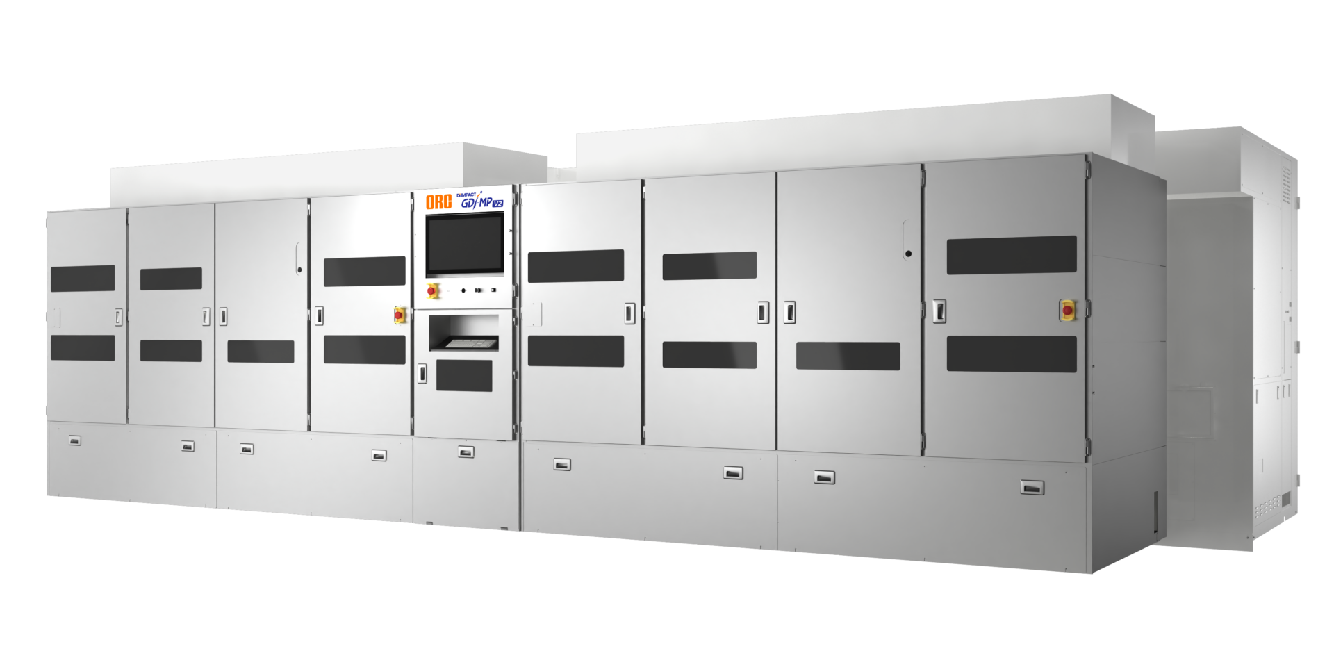
ORC Manufacturing is an equipment manufacturer which has forte in optical technologies, and its key product is direct imaging (Dl) system for production of high-density semiconductor packaging substrates. ORC Manufacturing is now developing next-generation Dl system for back-end processes of semiconductor packaging as a part of the project adopted by the New Energy and Industrial Technology Development Organization (NEDO). ORC Manufacturing’s participation in JOINT2 reinforces the consortium’s end-to-end testing line of leading-edge back-end process technologies. ORC Manufacturing’s Dl system, which does not require photo-mask preparation, is expected to shorten time-to-market of semiconductor packages, and accelerate technological innovations in back-end processes of semiconductor packaging.
Through its participation in JOINT2, ORC Manufacturing aims to acquire wide-ranging knowledge about back-end processes of semiconductor packaging including process evaluation technologies applicable to pre-imaging through post-imaging, thereby strengthen its capability to offer values to customers.

JOINT2 welcomes the new member, and will further promote open innovation and accelerate the development of more sophisticated evaluation technologies, materials, substrates, and equipment applicable to next-generation semiconductor packaging technologies.
[Comment by Norio Hashimoto, Chairman and CEO, ORC Manufacturing Co., Ltd.]
In sympathy with the JOINT2’s idea of “Co-creation”, we decided to join the consortium as a member in charge of “imaging technology to realize finer patterning.” ORC Manufacturing has been challenging to develop “unprecedented” optical-imaging technologies in order to realize more sophisticated semiconductor packages. We are now developing new DI system which can form circuit pattern with line width of 2µm or less, which will be applicable to advanced semiconductor packages. Through our future experience at JOINT2 in reliability evaluation of this system, we will strengthen our capability to suggest this tool to our customers and to meet our customers’ expectations.
About two years have passed since the launch of JOINT2, and we are now obtaining a variety of good results from our research. At ECTC (IEEE 73th Electronic Components and Technology Conference), we presented three major results of JOINT2’s research activities*4, and there was a huge good response from the audience. Now we are very happy to have ORC Manufacturing as a new member of JOINT2. The company has excellent optical imaging technology. ORC Manufacturing will strengthen the consortium’s capability to develop new technologies applicable to back-end processes of next-generation semiconductor package manufacturing. We are sure that JOINT2 consortium will continue bringing together world-class excellent companies, challenging to achieve ambitious targets of national projects, thereby leading development of technologies for back-end processes of semiconductor package manufacturing.
*2. 2.5D packaging refers to the technology of arranging parallel IC chips on a silicon interposer.
*3. 3D packaging refers to the technology of stacking chips using a through-silicon via (TSV).
*4. 1) Fine pitch bump bonding (the technology of vertically connecting IC chips and other components with high-density metal protrusions), 2) Fine pitch redistribution layer (RDL) formation (the technology of connecting IC chips and other components in a planar direction with high-density circuit), 3) Highly reliable large-substrate manufacturing technology which realizes mounting of large components.