December 02, 2024
Resonac Corporation (President: Hidehito Takahashi, hereinafter referred to as “Resonac”) has developed a new high-resolution photosensitive film for use in the manufacturing of advanced semiconductors, such as AI processors. This film enables the formation of ultra-fine copper circuits with a line width and spacing of 1.5 micrometers (μm) on organic interposers*1. (Patent acquired)
Semiconductors have evolved to integrate more functions on a single integrated circuit by miniaturizing circuits, allowing for complex computational processing at high speeds. In recent years, packaging technologies have continued to innovate, including chiplet technology*2 which interconnects multiple chips on an interposer to achieve both high functionality and high-speed processing.
Currently, interposers are manufactured using wafers, but as the number of chips increases, the interposer area needs to be enlarged, presenting challenges such as yield rates. As a solution, organic interposers, which are produced using organic materials and copper plating in a square panel with a side length of about 500 to 600 millimeters, have gathered attention. The newly developed photosensitive film by Resonac achieves a resolution of 1.5 μm in both line width and spacing for organic interposers. The product is provided in a film type suitable for the panel manufacturing process.

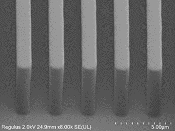
Resist pattern
(Line width of resist: 1.5μm / Spacing: 1.5μm)

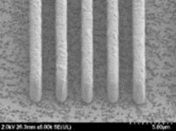
Formed copper plating pattern
(Line width of copper plating: 1.5μm / Spacing: 1.5μm)

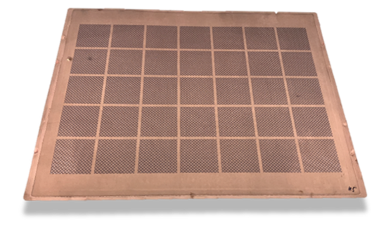
Panel with formed copper plating wiring
(Line width of copper plating: 1.5μm / Spacing: 1.5μm)
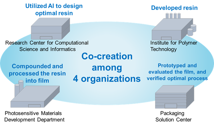
In the development process, co-creation was carried out by four organizations. This time, we developed a new polymer resin that is key to achieving the required high resolution. In this development, we utilized AI technology provided by the Research Center for Computational Science and Informatics to perform optimal resin design, while the Institute for Polymer Technology was responsible for the actual resin development. Furthermore, the Photosensitive Materials Development Department conducted the formulation and film processing using this resin. Finally, the Packaging Solution Center*3 conducted prototype testing and evaluation of copper wiring on panels using this film, verifying the optimal process.

Resonac will continue developing and providing cutting-edge materials to support the evolution of semiconductors for the next generation.
*1. Interposer: A component used to interconnect multiple chips.
*2. Chiplet technology: A technology that mounts and interconnects multiple types of chips, such as those manufactured with cutting-edge processes and those with conventional processes, on an interposer to enable them to function together.
*3. Packaging Solution Center: A research and development hub dedicated to packaging and evaluation technologies, equipped with a full lineup of state-of-the-art back-end processing equipment.